Read Write Processor Bus Cycles
Embedded software developers working in fault tolerance of the system work close to the underlying hardware. Thus a basic understanding of hardware operation is useful in developing software that interfaces directly with the hardware. In this article we will focus on some basic processor bus cycles. Understanding of bus cycle operations is useful in designing diagnostics and exception handlers.
The following processor bus cycles are described in detail:
| Read Bus Cycle | Describes the operations carried out by the processor when a memory read is executed. |
| Write Bus Cycle | Sequence of operations in memory write is described here. |
| Bus Error | Processor initiates a bus cycle, but memory subsystem does not find the addressed memory location. |
| Read-Modify-Write Bus Cycle | This bus cycle is used to perform locking operations in a multiprocessor system. This is an atomic read followed by write operation. |
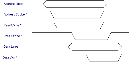
Read Bus Cycle

- Processor initiates a read bus cycle by floating the address of the memory location on the address lines.
- Once the address lines are stable, the processor asserts the address strobe signal on the bus. The address strobe signals the validity of the address lines.
- Processor then sets the Read/Write* signal to high, i.e. read.
- Now the processor asserts the data strobe signal. This signals to the memory that the processor is ready to read data.
- The memory subsystem decodes the address and places the data on the data lines.
- The memory subsystem then asserts the data acknowledge signal. This signals to the processor that valid data can now be latched in.
- Processor latches in the data and negates the data strobe. This signals to the memory that the data has been latched by the processor.
- Processor also negates the address strobe signal.
- Memory subsystem now negates the data acknowledgement signal. This signals the end of the read bus cycle.
Write Bus Cycle
- Processor initiates a write bus cycle by floating the address of the memory location on the address lines.
- Once the address lines are stable, the processor asserts the address strobe signal on the bus. The address strobe signals the validity of the address lines.
- Processor then sets the Read/Write* signal to low, i.e. write.
- The processor then places the data on the data lines.
- Now the processor asserts the data strobe signal. This signals to the memory that the processor has valid data for the memory write operation.
- The memory subsystem decodes the address and writes the data into the addressed memory location.
- The memory subsystem then asserts the data acknowledge signal. This signals to the processor that data has been written to the memory.
- Then the processor negates the data strobe, signaling that the data is no longer valid.
- Processor also negates the address strobe signal.
- Memory subsystem now negates the data acknowledgement signal, signaling an end to the write bus cycle.
Bus Error
Here we cover the example of a read bus cycle that fails due to the address being accessed was illegal. The processor aborts the bus cycle and initiates exception processing.
- Processor initiates a read bus cycle by floating the address of the memory location on the address lines.
- Once the address lines are stable, the processor asserts the address strobe signal on the bus. The address strobe signals the validity of the address lines.
- Processor then sets the Read/Write* signal to high, i.e. read.
- Now the processor asserts the data strobe signal. This signals to the memory that the processor is ready to read data.
- The memory subsystem decodes the address but finds that there is no memory corresponding to the address.
- The memory subsystem, then asserts the bus error signal. This signals to the processor that an illegal address access has been attempted.
- Processor aborts the current bus cycle and initiates bus error exception processing.
- The current processor context is saved and the processor moves to supervisor mode.
- The processor then fetches the bus error vector to obtain the address of the bus error handler.
- Control is then transferred to the bus error handler.
Read-Modify-Write Bus Cycle
A read-modify-write bus cycle is nothing but a read cycle followed by a write cycle to the same address. This bus cycle is important when designing multiprocessor systems. Since the read and write operations are performed in a single bus cycle, the processor cannot loose the bus when these operations are being carried out. This type of bus cycle is used when dealing with resources managed by semaphores.
- Processor initiates read-modify-write bus cycle by floating the address of the memory location on the address lines.
- Once the address lines are stable, the processor asserts the address strobe signal on the bus. The address strobe signals the validity of the address lines.
- Processor then sets the Read/Write* signal to high, i.e. read.
- Now the processor asserts the data strobe signal. This signals to the memory that the processor is ready to read data.
- The memory subsystem decodes the address and places the data on the data lines.
- The memory subsystem, then asserts the data acknowledge signal. This signals to the processor that valid data can now be latched in.
- Processor latches in the data and negates the data strobe. This signals to the memory that the data has been latched by the processor.
- Memory subsystem now negates the data acknowledgement signal, signaling an end to the read part of the bus cycle.
- Processor then sets the Read/Write* signal to low, i.e. write.
- The processor then places the data on the data lines.
- Now the processor asserts the data strobe signal. This signals to the memory that the processor has valid data for the memory write operation.
- The memory subsystem decodes the address and writes the data into the addressed memory location.
- The memory subsystem then asserts the data acknowledge signal. This signals to the processor that data has been written into the memory.
- Then the processor negates the data strobe, signaling that the data is no longer valid.
- Processor also negates the address strobe signal.
- Memory subsystem now negates the data acknowledgement signal, signaling an end to the read-modify-write bus cycle.